It is well known that dimensional confinement of electrical carriers in materials enhances electronic correlations, leading to exotic properties that cannot be understood by semiclassical models: low dimensionality is ruled by the realm of quantum mechanics. This fact has been widely recognized in two dimensional systems such as graphene, 2D transition metal dichalcogenides, and thin films and heterostructures of a variety of materials. The family of transition metal chalcogenides (TMCs) are widely-known low-dimensional materials used in many fields of physics and material science. They show interesting fundamental ground states, as well as great promise for their use in optic and electronic devices. These are low-dimensional materials with general chemical formula MXn, with n=2,3,4,…, where M is a transition metal (Mo, Nb, Ta, Hf, among others) and X a chalcogen atom (S, Se or Te). Atoms in this structure are strongly-bonded either in a plane (for the case of the 2D dichalcogenides MX2) or an axis (for the case of the quasi-1D tri- and tetra-chalcogenides, MX3 and MX4), and weakly bonded and stacked by van-der-Waals forces in the other directions. This last characteristics gives them their low-dimensionality character, and furtheremore, allows the isolation of single- or few-atomic-layers-thick samples through relatively simple mechanical exfoliation techniques. Their visible or near-visible range bandgaps, elevated electronic mobilities, large spin-orbit interaction, large susceptibility to changes in physical parameters, spatial scalability, among other characteristics, makes them ideal candidates for a large number of aplications. In addition, depending on the chemical composition they can be semiconductors, semimetals, metals or topological insulators, and they can show charge density wave (CDW) ordering, superconductivity and/or magnetic properties. Additionally, this family of materials exhibits a strong susceptibility of the electronic and physical properties to the tuning of control parameters such as chemical doping, pressure, electrostatic doping, strain or thickness. This allows to easily varying the critical temperature of phase transitions, which makes them ideal systems for the studies of quantum criticality and optimization of electronic properties.
Having these materials as a playground for novel physics, in our group we are interested in studying topics such as:
|
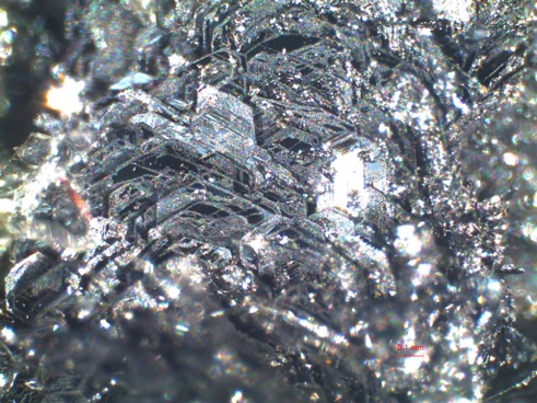 Image: Collection of NbTe2 single crystals grown by our group. Image: Collection of NbTe2 single crystals grown by our group. |
Some examples of materials we are currently investigating, and for which we are using chemical doping to vary their electronic properties, are the dichalcogenides TaS2, NbTe2, WSe2 and WTe2; the trichalcogenides NbSe3 and HfTe3; the tetrachalcogenides NbTe4 and TaTe4; the pentachalcogenides HfTe5 and ZrTe5; among others.
We use a combination of transport measurements, thermodynamic measurements (RUS), magnetic measurements, X-ray diffraction and microscopy measurements to characterize these and the other materials we synthesize and study. We also commonly use tuning parameters such as temperature and magnetic field to study the properties of these systems, and many times need to acces extreme conditions such as temperatures down to 1K or magnetic fields up to 45 T or even 100 T (typically at the National High Magnetic Field Laboratory in USA) to reveal the quantum secrets of these compounds.